Author: DAHENG IMAGING Date: 2021-07-23
Industry: Photovoltaic
Project: Electroluminescence (EL) Detection
Background
At present, the third energy revolution makes the global energy structure gradually transform to renewable energy. Solar energy as a clean energy with great potential, is getting more and more attention. Photovoltaic (PV) panels are devices that use the photoelectric conversion principle to convert solar radiation energy directly or indirectly into electrical energy. Most PV cells currently use silicon material as the substrate, which can be divided into crystalline silicon cells and amorphous silicon cells.
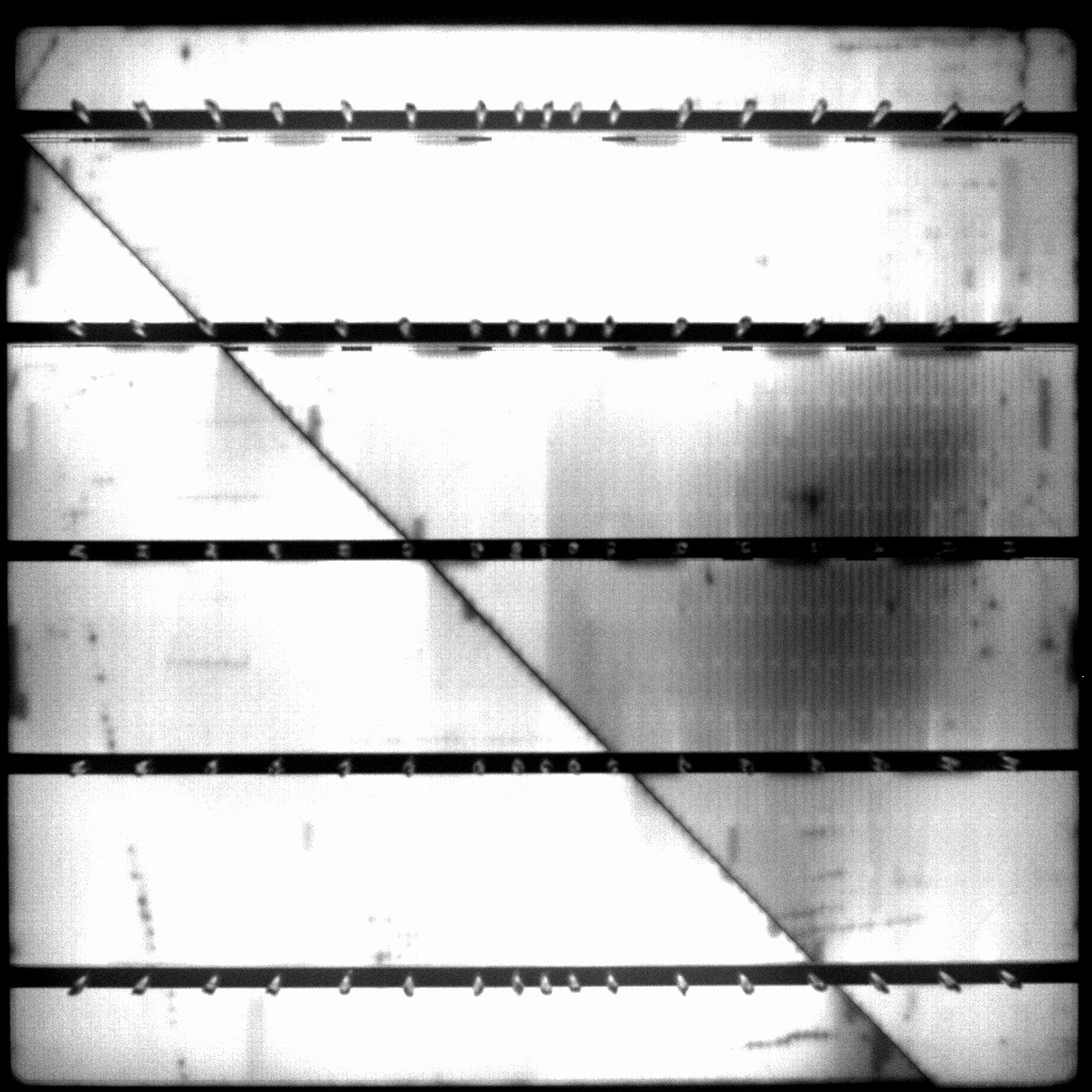
Some structural defects such as micro-cracks, finger-interruption, contamination or cell inter-connection degradation may occur during silicon processing, which are influenced by lattice quality or other conditions, and that may decrease the power efficiency of solar modules. Conventional imaging systems are particularly difficult to identify these defects, so it’s necessary to use electroluminescence (EL) imaging to detect defects such as hidden cracks, break, black-fleck, belt marks, and diffusion anomalies in cells.
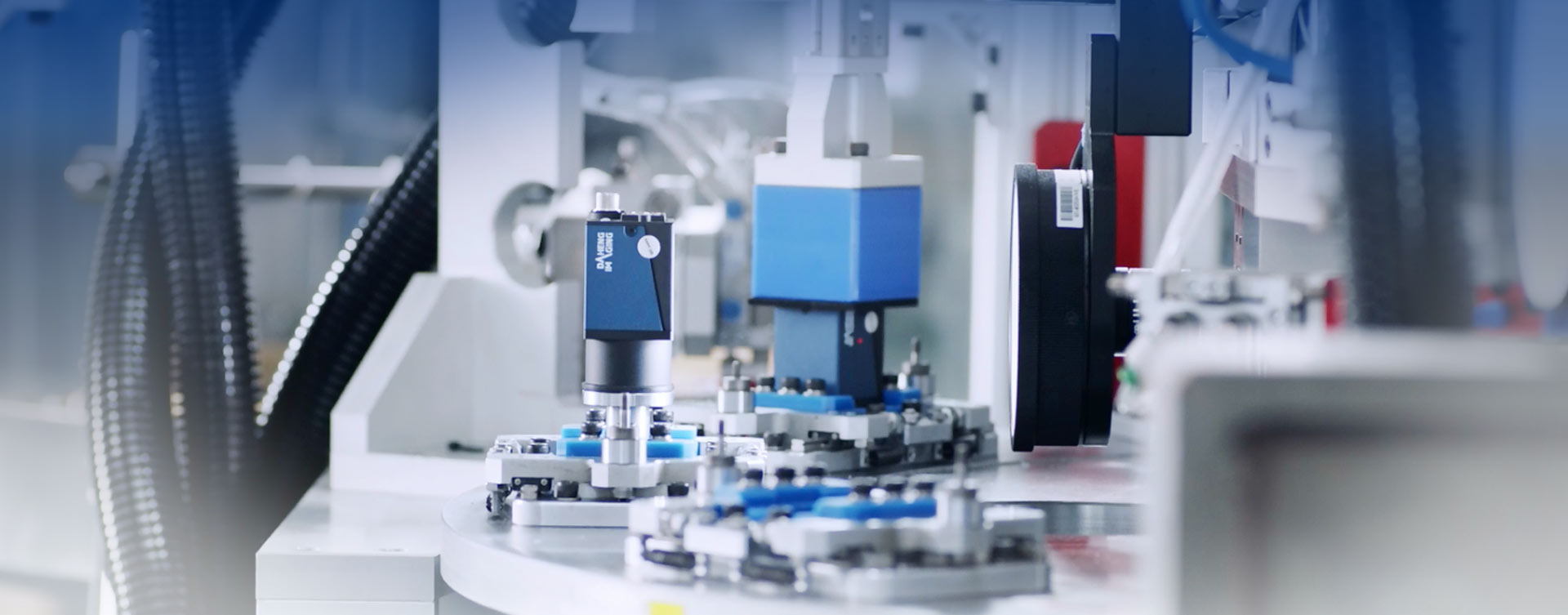
Program Overview:
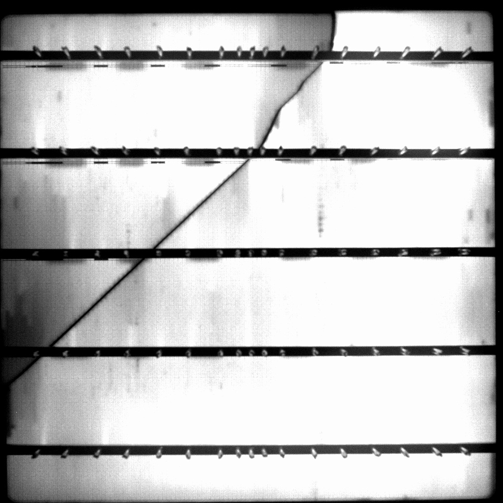
EL is a phenomenon that converts electrical energy into optical energy. Inter-band complex luminescence occurs within the inner material by applying a voltage to the material. For silicon materials, the peak of the luminescence spectrum corresponds to 1110 nm, and the width of the inter-band complex is between 1000 and 1300 nm. In the obtained images, the active regions of normal panels with good conductivity have higher luminance and relatively uniform luminance distribution, but the inactive regions and poor contact areas have lower luminance. High-sensitivity NIR cameras are needed for EL detection because the electroluminescence in the panels is very weak.

Solution
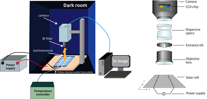
EL detection schematic
Applications: Finished battery slice, module products
Process Location: Currently, the most common installation location is after string welding, tile stacking, or the finished module. Usually it is installed after the finished cell or before string welding, depending on the customer's needs.
Presentation
 |  |  | ||
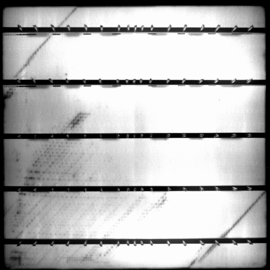 | 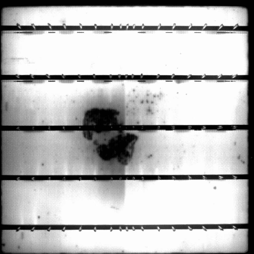 |  |
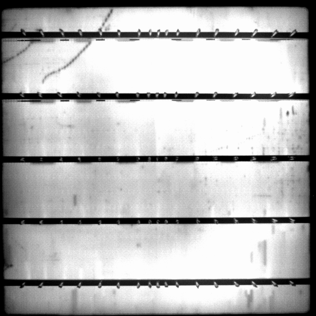
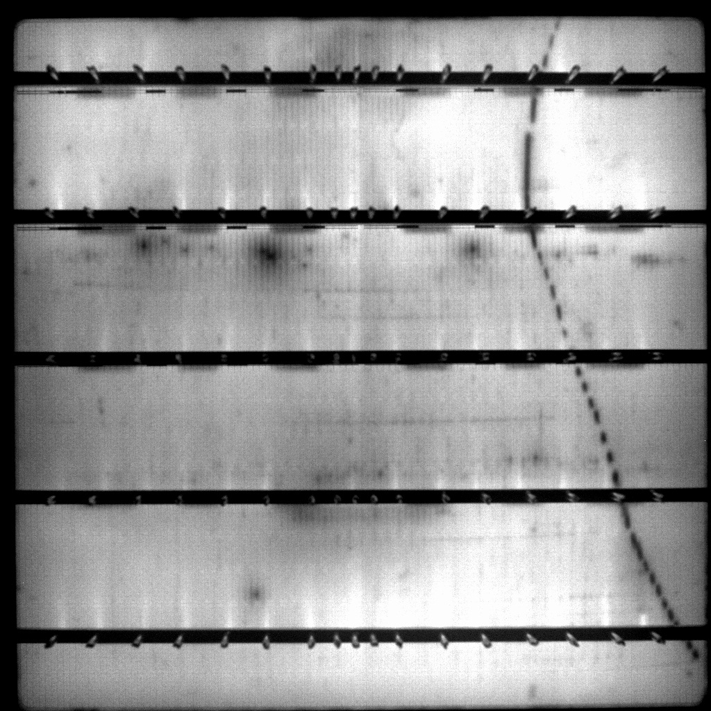
Defect images
 | 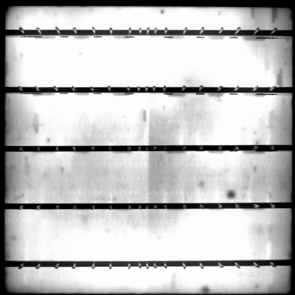 | |
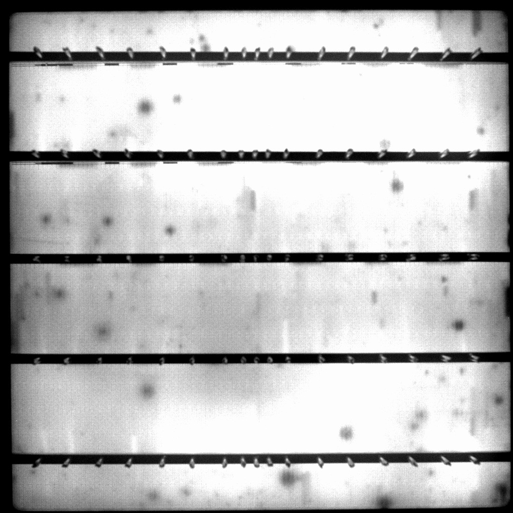 | 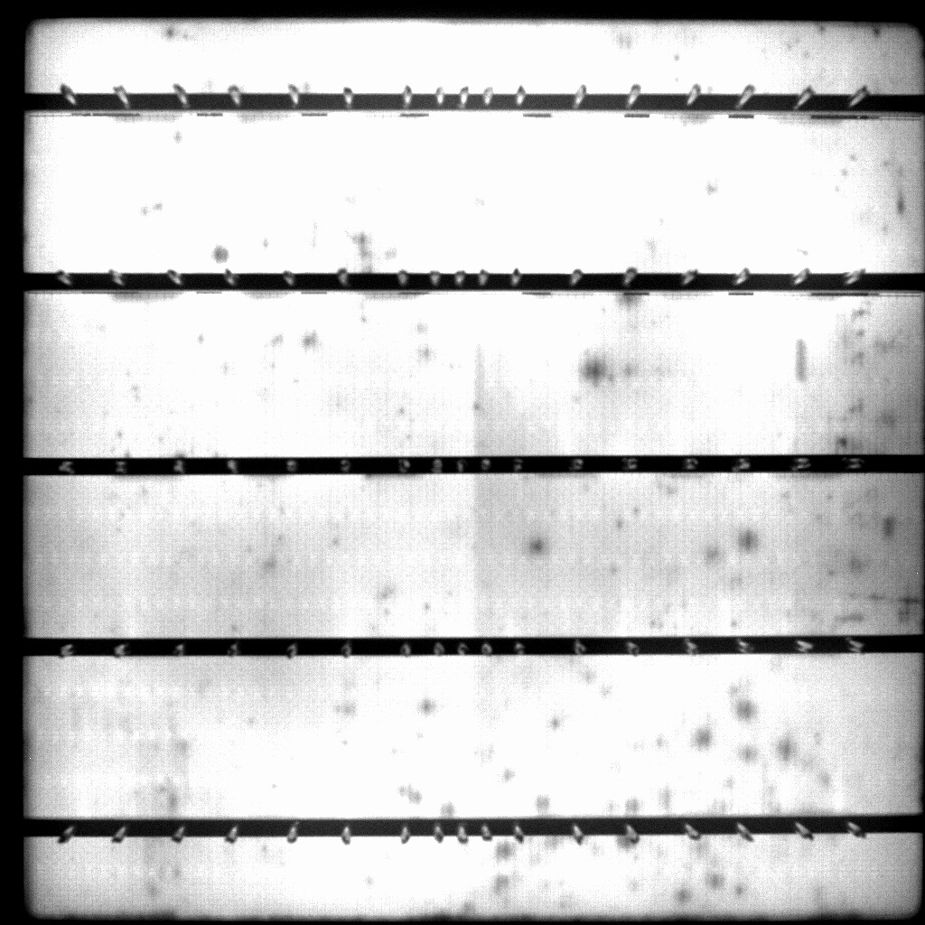 |
Normal images
Related Products
 |  |
Address:12F Daheng Science & Technology Tower, No.3 Suzhou Str., Haidian District, Beijing China
E-mail:isales@daheng-imaging.com