Author: DAHENG IMAGING Date: 2021-07-24
Industry: Photovoltaic
Project: Photoluminescence (PL) Detection
Background
Photovoltaic industry has developed rapidly in recent years. In order to pursue higher efficiency and reduce production costs, production process and technology is also progressing and developing. During the production of photovoltaic panels, problems such as hidden cracks, uneven diffusion and void may occur. These defects may affect the photovoltaic conversion efficiency, reduce the life of the cell and affect the stability of the Photovoltaic system. Photoluminescence (PL) inspection can realize the detection and analysis of various processes such as silicon wafer, diffusion, etching, electrode printing and cell wafer. It can quickly and effectively locate problems in the production process and provide reliable assurance for product quality.
Solution
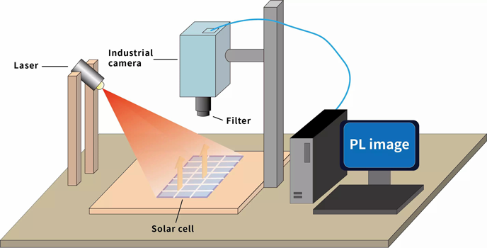
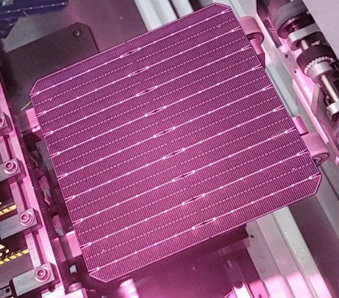
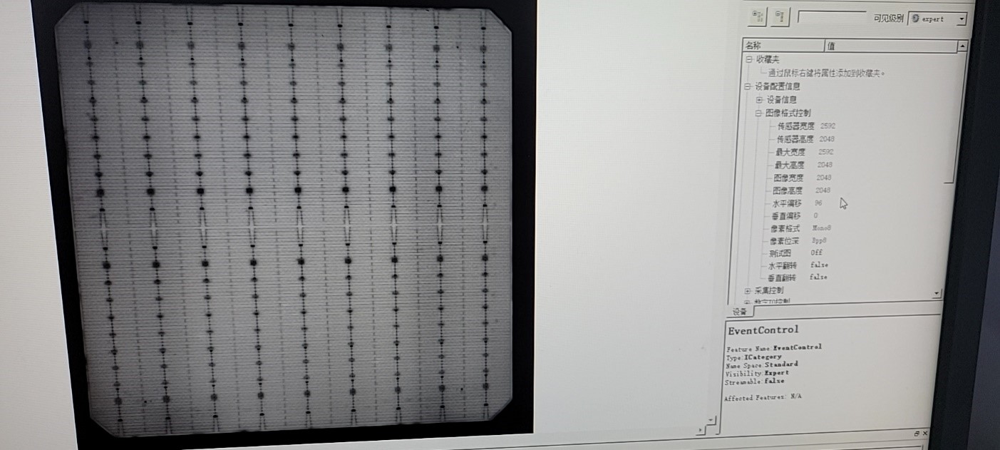
Photoluminescence principle: Using a laser of a specific wavelength as the excitation light source to provide photons of a certain energy. The ground state electrons in the silicon wafer absorb these photons and transfer into the excited state, releasing near-infrared light with a wave peak around 1150 nm. Then use a high sensitive and high resolution camera for light sensing and imaging. The intensity of light after imaging is proportional to the concentration of non-equilibrium minority carriers at the corresponding position, and the minority carrier concentration in the region is reduced due to defects, thus weakening the fluorescence effect. After imaging, it appears as dark dots, lines or certain areas. Therefore, the photoluminescence can be used to determine whether the sample has defects, impurities and other factors that ultimately affect the efficiency of the cell.
Application: Silicon ingots, wafers, process wafers, solar cell wafers, module products
Process position: After string welding, tile stacking or a finished product, usually it is also installed according to the customer's needs——after the battery cells finished, or before the string welding loading. It is also adapt to the upstream industry, such as silicon wafer and silicon ingot testing.
Advantages
1) No contact, no secondary defects.
2) High detection efficiency.
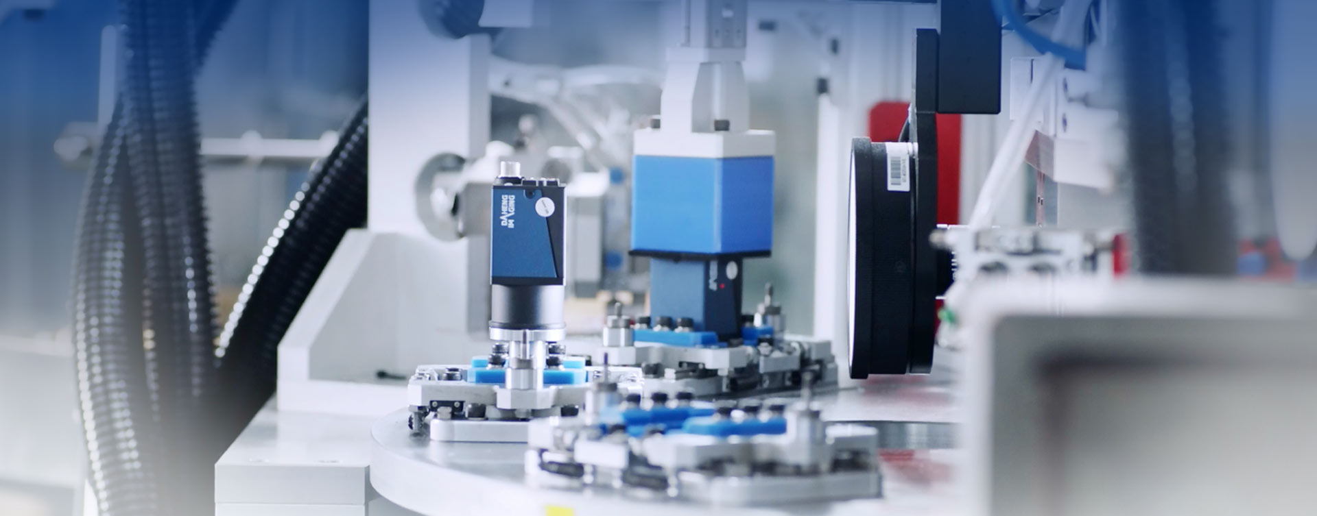
Presentation
Related Products
 |  |
Address:12F Daheng Science & Technology Tower, No.3 Suzhou Str., Haidian District, Beijing China
E-mail:isales@daheng-imaging.com