
Author: DAHENG IMAGING Date: 2021-10-18
Industry: Semiconductor
Project: Lead frame vision inspection system
Background
As a special material for semiconductor and microelectronic packaging, lead frame used to make an electrical connection between the internal circuit lead port (bonding point) of the chip and the external lead, with the help of bonding materials (gold wire, aluminum wire, copper wire). Lead frame is the key structural part to form the electrical circuit. As a connection between the internal circuit and external circuit, lead frame plays the role of stabilizing the chips, conducting signals and transmitting heat.
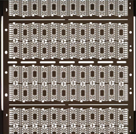
Lead frame
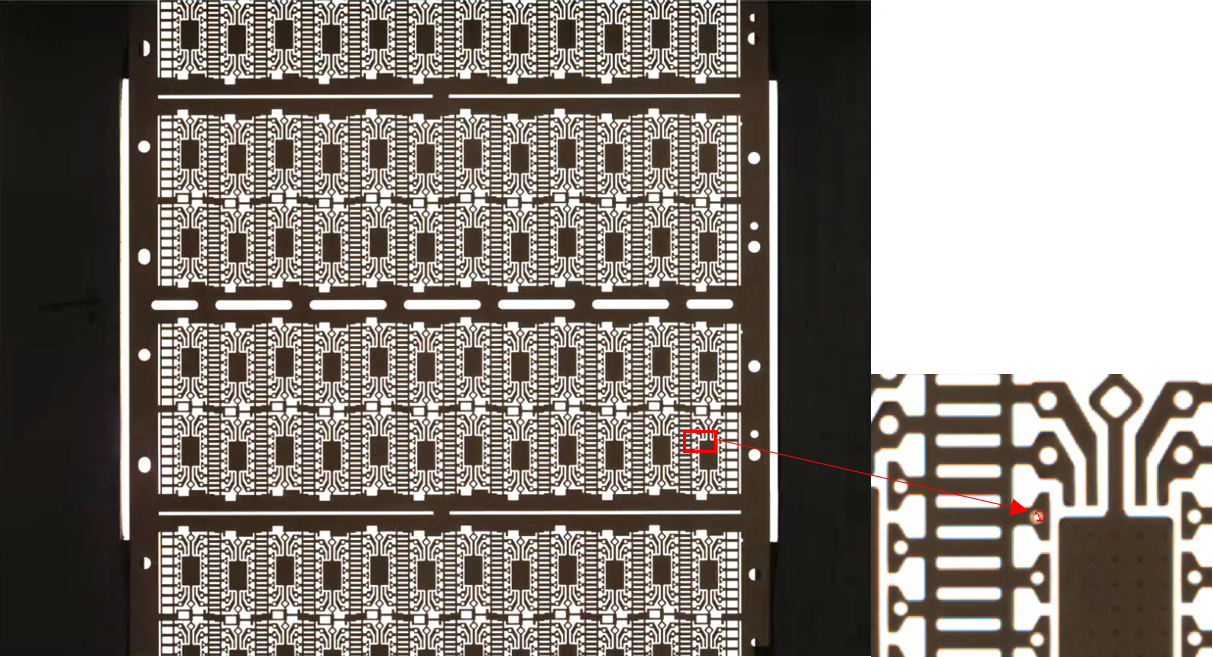
As a key part of the semiconductor packaging, the lead frame needs to meet high standards in terms of coplanarity, strength, bending, etc. Its quality will directly affect the quality of the semiconductor packaging. However, during the process of production, defects such as false punching, miss punching, smudge, oxidation, burring, crushing, deformation, miss plating and false plating will inevitably occur due to various factors. Along with the miniaturization of today's chip packaging, the introduction of machine vision inspection systems into the assembly line can effectively improve product qualification rates and reduce production costs and time.
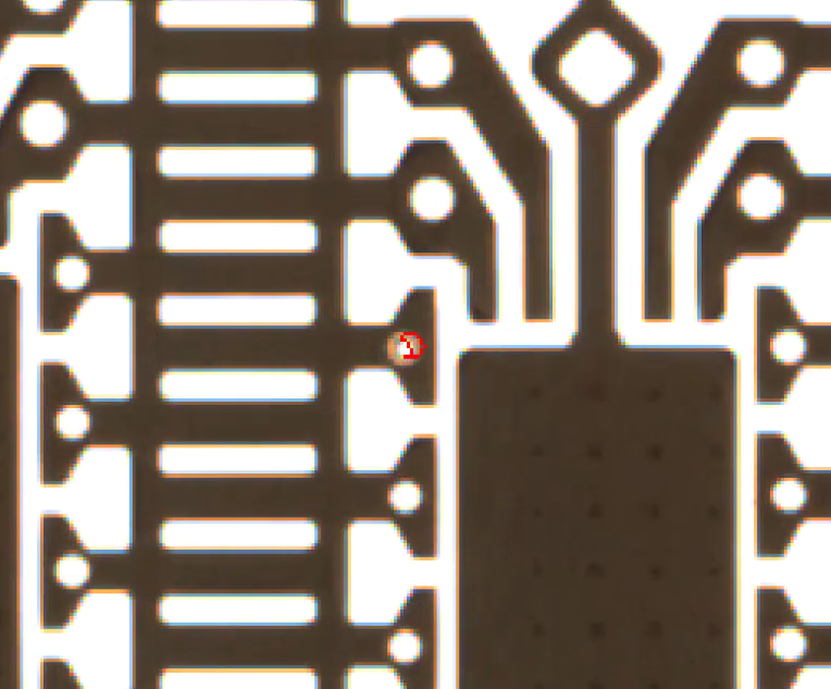 |  | 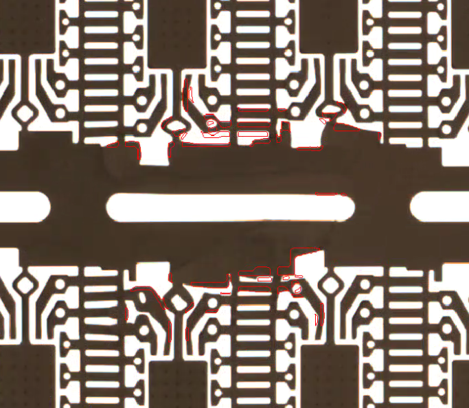 | ||
Miss punching | Smudge | Deformation |
Difficulties
1) At present, most of the domestic chip packaging defect detection technologies are remain at the stage of manual detection or semi-automatic detection, with low detection efficiency and unsecured detection quality.
2) The lead frame size is relatively small and flat.
3) The assembly line have a high density of product placement.
4) The testing environment is heavily influenced by machinery.
Solution
Hardware Selection: MER-503-36U3C Industrial Camera
Global shutter can reduce the vibration effects caused by environmental issues. Considering it may exists erythema defects on the product surface at the meantime, choose color cameras can meet the needs of algorithmic detection.
Software: C# + HALCON
C# WINFORM interface can meet the customer's rapid development needs, and the interface style is relatively flexible. It is also free to choose for customers. HALCON algorithm library is fast, robust and rich in operators, which can shorten the software development cycle.
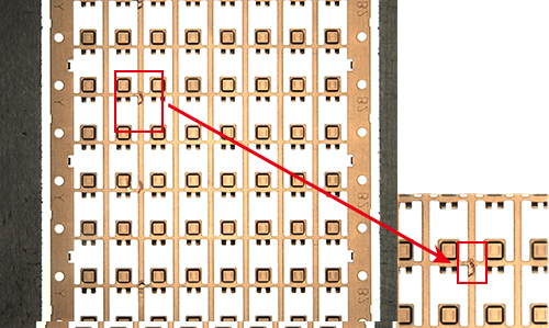
Presentation
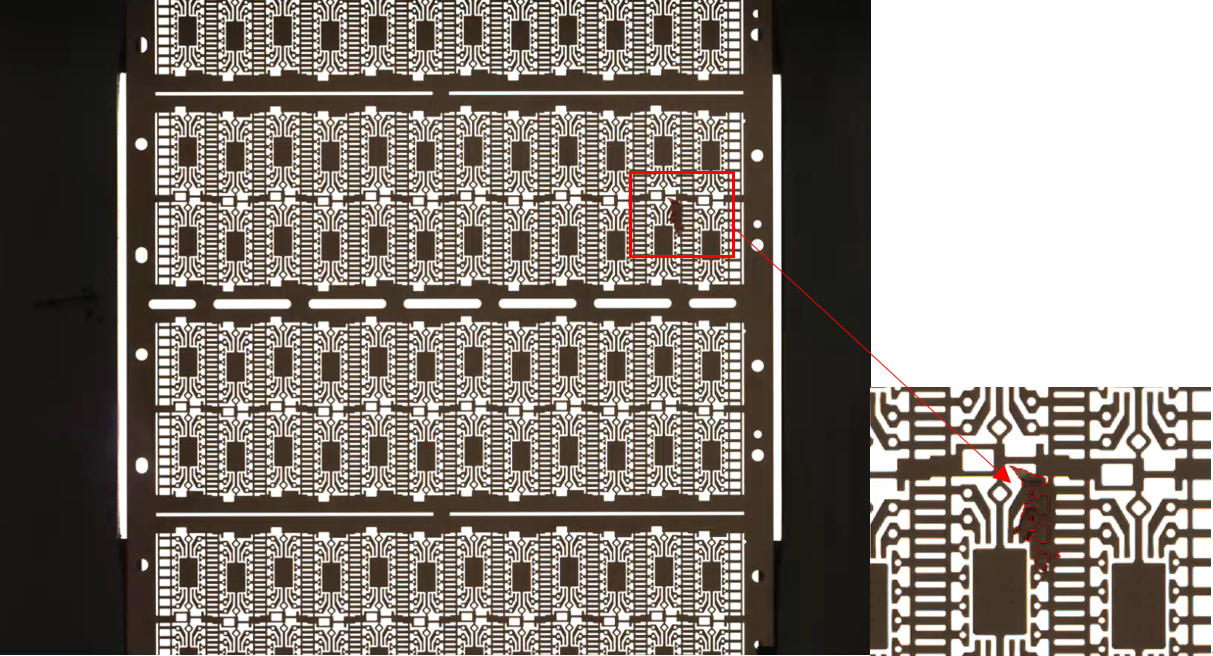
 | 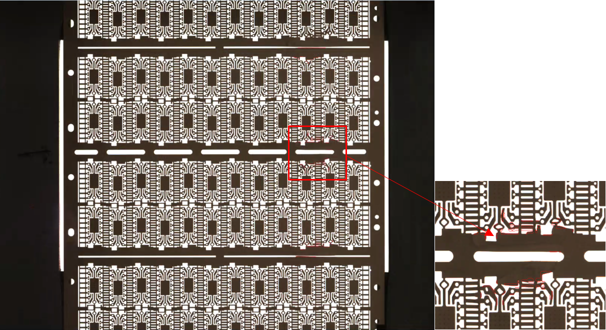 | |
Miss-punching | Deformation | |
 |  | |
Scraps 1 | Scraps 2 |
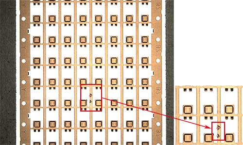 | 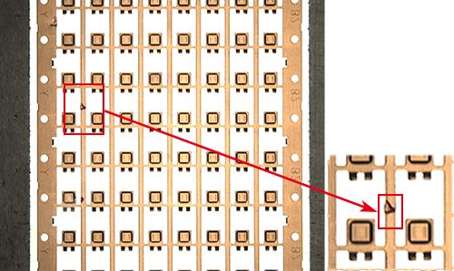 |  | ||
Crushing 1 | Crushing 2 | Crushing 3 |
Related Products

Address:12F Daheng Science & Technology Tower, No.3 Suzhou Str., Haidian District, Beijing China
E-mail:isales@daheng-imaging.com